

Thin-film Lithium Niobate
Lithium niobate (LN) , which demonstrated its exceptional performance in fiber-optic communications over the past decade, has become the material of choice in high-performance electro-optic modulators. Despite having various preferable performance in optical communication, traditional bulky LN modulators have its limitations in integration size, power consumption,Vπ and so forth. To overcome these limitations, Ori-Chip has developed cutting-edge thin-film lithium niobate (TFLN) technologies1-3. Ori-Chip TFLN modulators have demonstrated superior performance including: miniaturization of chip length, >20dB extinction ratio (ER), <3.3V Vπ and so forth. These preferable properties make TFLN modulators an ideal solution for the next generation high-speed optical communication systems. Figure 1 shows a photograph of a 4-inch TFLN wafer fabricated in-house from Ori-Chip wafer fab.

Figure 1. Photograph of a 4-inch Ori-Chip TFLN wafer
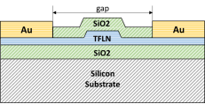
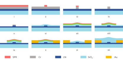
Figure 2 (a) shows the cross-sectional image of the completed TFLN modulator. Integrated with co-planar wave (CPW) traveling-wave electrode, the x-cut TFLN modulator is able to realize push-pull modulation naturally. Figure 2 (b) shows the schematic diagram of the process flow of fabricating the TFLN modulator. First, Waveguides are defined by photolithography. Inductively coupled plasma (ICP) etcher is subsequently used to transfer the photoresist pattern onto the Cr mask. After photoresist removal, an optimized ICP dry etching process is employed for LN etching. Etch depth is accurately controlled in this process. Then, a layer of silica is deposited on the waveguide by plasma enhanced chemical vapor deposition (PECVD). After this, part of the the silica layer is etched by ICP dry etching before the electrode pattern is defined by PMGI and SPR photoresist. Followed by TWE formation by Au evaporation and lift-off, the deposition of a protective layer of silica completes the process. Figure 3 shows the scanning electron microscope (SEM) image of an etched TFLN modulator
(a)
(b)
Figure 2. (a) Cross-sectional image of the TFLN modulator; (b) Schematic diagram of the process flow of TFLN modulator
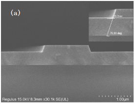
Figure 3. SEM image of an etched TFLN modulator
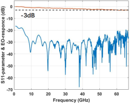
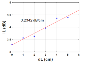
Measured S-parameters and insertion loss (IL) on a TFLN modulator chip are shown in Figure 4 (a)-(b). Results indicate that Ori-Chip TFLN modulators are able to achieve wide modulation bandwidth and low insertion loss at the same time.
(a)
(b)
Figure 4. (a) S-parameters (b) IL measured on a TFLN modulator chip
[1] H. Li, Y. Liu, J. Liu, S. Tan, Q. Lu, M. Lu, and W. Guo, "Low Vπ silicon-based x-cut thin-film lithium niobate MZ modulators fabricated by photolithography," in Asia Communications and Photonics Conference/International Conference on Information Photonics and Optical Communications 2020 (ACP/IPOC), K. Xu, D. Simeonidou, C. Chang-Hasnain, N. Wada, X. Ren, Z. Zhukov, P. Perry Shum, Y. Ji, J. Zhang, X. Zhou, C. Lu, and L. Wosinska, eds., OSA Technical Digest (Optical Society of America, 2020), paper S4D.4.
[2] H. Li, Q.Chen, Y. Liu, Y.Tang, Q. Lu, M. Lu, and W. Guo, “High performance thin-film lithium niobate MZ modulator ready for massive production,” in Optical Fiber Communication Conference 2022 (OFC).
[3]Ye Liu, Heng Li, Jia Liu, Su Tan, Qiaoyin Lu, and Weihua Guo, "Low Vπ thin-film lithium niobate modulator fabricated with photolithography," Opt. Express 29, 6320-6329 (2021)


